
 Datasheet下载
- 型号: FHS 40-P/SP600
- 制造商: LEM
- 库位|库存: xxxx|xxxx
- 要求:
| 数量阶梯 | 香港交货 | 国内含税 |
| +xxxx | $xxxx | ¥xxxx |
查看当月历史价格
查看今年历史价格
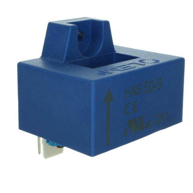
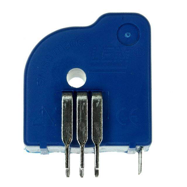
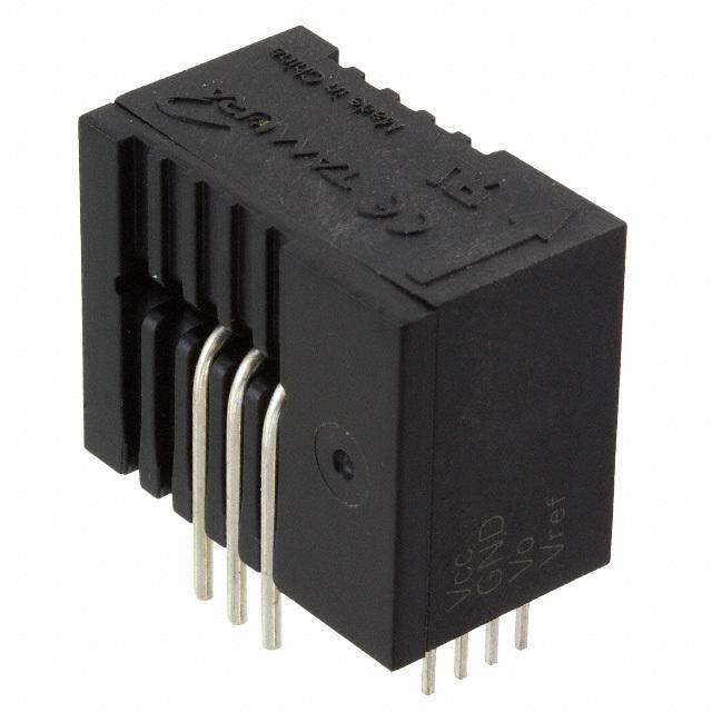
FHS 40-P/SP600产品简介:
ICGOO电子元器件商城为您提供FHS 40-P/SP600由LEM设计生产,在icgoo商城现货销售,并且可以通过原厂、代理商等渠道进行代购。 FHS 40-P/SP600价格参考¥60.00-¥72.00。LEMFHS 40-P/SP600封装/规格:电流变送器, Current Sensor 100A 1 Channel Hall Effect, Open Loop Bidirectional 8-SOIC (0.154", 3.90mm Width)。您可以下载FHS 40-P/SP600参考资料、Datasheet数据手册功能说明书,资料中有FHS 40-P/SP600 详细功能的应用电路图电压和使用方法及教程。
LEM USA Inc. 的 FHS 40-P/SP600 是一款开环式电流变送器,主要用于工业自动化和电力电子系统中对直流、交流或脉冲电流的高精度测量与监控。该型号额定电流为 ±40A,具备良好的线性度和温度稳定性,输出信号为比例电压,便于与控制系统集成。

典型应用场景包括:
1. 变频驱动系统:用于电机控制中实时监测电流,提高能效与运行稳定性;
2. 不间断电源(UPS)与逆变器:在电能转换过程中实现过流保护与闭环控制;
3. 可再生能源系统:如太阳能逆变器和风力发电变流器,用于直流侧和交流侧电流检测;
4. 工业电源与焊接设备:精确测量大电流输出,确保工艺质量与设备安全;
5. 电动汽车充电设施:在充电桩或车载电源系统中进行电流监控,保障充电过程安全可靠。

FHS 40-P/SP600 采用紧凑型设计,绝缘性能优良,适用于空间受限且要求高可靠性的环境。其非接触式测量原理减少了能量损耗,提升了系统整体效率。广泛应用于需要高隔离电压、强抗干扰能力和长期稳定性的工业与能源领域。
| 参数 | 数值 |
| 产品目录 | |
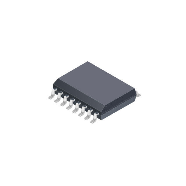
| 描述 | SENSOR CURRENT 100A 5V BI 8SOIC |
| 产品分类 | |
| 品牌 | LEM USA Inc |
| 数据手册 | |
| 产品图片 |
|
| 产品型号 | FHS 40-P/SP600 |
| rohs | 无铅 / 符合限制有害物质指令(RoHS)规范要求 |
| 产品系列 | FHS |
| 产品培训模块 | http://www.digikey.cn/PTM/IndividualPTM.page?site=cn&lang=zhs&ptm=1401 |
| 产品目录页面 | |
| 传感器类型 | 霍尔效应, 开环 |
| 其它名称 | 398-1057-1 |
| 包装 | 剪切带 (CT) |
| 响应时间 | 3µs |
| 安装类型 | 表面贴装 |
| 封装/外壳 | 8-SOIC(0.154",3.90mm 宽) |
| 工作温度 | -40°C ~ 125°C |
| 极化 | 双向 |
| 标准包装 | 1 |
| 灵敏度 | 600mV/mT |
| 特色产品 | http://www.digikey.com/cn/zh/ph/lem/mini.html |
| 用于测量 | AC/DC |
| 电压-电源 | 4.75 V ~ 5.5 V |
| 电流-检测 | 100A |
| 电流-电源(最大值) | 20mA |
| 精度 | - |
| 线性度 | ±0.4% |
| 输出 | 比率, 电压 |
| 通道数 | 1 |
| 配用 | /product-detail/zh/FHS%2040-P%20KIT%209-1P/398-1069-ND/1680536/product-detail/zh/FHS%2040-P%20KIT%208-1P/398-1070-ND/1680537/product-detail/zh/FHS%2040-P%20KIT%207-1P/398-1071-ND/1680538/product-detail/zh/FHS%2040-P%20KIT%206-1P/398-1072-ND/1680539/product-detail/zh/FHS%2040-P%20KIT%205-1P/398-1073-ND/1680540/product-detail/zh/FHS%2040-P%20KIT%204-1P/398-1074-ND/1680541 |
| 频率 | 105kHz |


- 商务部:美国ITC正式对集成电路等产品启动337调查
- 曝三星4nm工艺存在良率问题 高通将骁龙8 Gen1或转产台积电
- 太阳诱电将投资9.5亿元在常州建新厂生产MLCC 预计2023年完工
- 英特尔发布欧洲新工厂建设计划 深化IDM 2.0 战略
- 台积电先进制程称霸业界 有大客户加持明年业绩稳了
- 达到5530亿美元!SIA预计今年全球半导体销售额将创下新高
- 英特尔拟将自动驾驶子公司Mobileye上市 估值或超500亿美元
- 三星加码芯片和SET,合并消费电子和移动部门,撤换高东真等 CEO
- 三星电子宣布重大人事变动 还合并消费电子和移动部门
- 海关总署:前11个月进口集成电路产品价值2.52万亿元 增长14.8%


PDF Datasheet 数据手册内容提取
Current transducer FHS 40-P/SP600 I = 0 - 100 A PM Minisens Introduction The Minisens transducer is an ultra flat SMD open loop integrated circuit current transducer based on the Hall effect principle. It is suitable for the electronic measurement of currents: DC, AC, pulsed, mixed. It has no insertion loss and provides galvanic isolation between the primary circuit (high power) and the secondary circuit (sensor). It measures the magnetic field generated by the current flowing in a conductor such as a PCB track. The output voltage is proportional to that magnetic field. The IC is calibrated to minimize offset and temperature drifts. An integrated magnetic circuit gives an optimum transducer sensitivity. High isolation between the primary circuit and transducer electronics can be obtained with a double sided PCB. This datasheet is for a device programmed for maximum sensitivity: other options will be available. For example, the sensitivity range will be adjustable, and a choice of fixed or ratiometric (proportional to power supply voltage) sensitivity and reference voltage will be offered. Features Applications ● Programmable Hall effect transducer for current ● Battery supplied applications ● Motor control measurement applications up to ± 100 A ● Power meter ● 5 V power supply ● Uninterruptible Power Supplies (UPS) ● Standard S0IC 8 pin package ● Switched Mode Power Supplies (SMPS) ● Overcurrent fault protection ● Magnetic field measurement range ± 3.3 mT ● Threshold detection ● Sensitivity range up over to 200 mV/A ● Garage door opener ● Isolated current measurement. ● Window shutters ● Motors and fans Advantages ● Air conditioning ● White goods. ● Low cost ● Small size Application domain ● Excellent linearity ● Industrial. ● No power loss in primary circuit ● Internal or external reference voltage may be used on Standard the same pin ● EN 50178. ● Standby mode for reduced power consumption ● Additional output for fast detection with response time 3 µs. Page 1/18 100727/10 LEM reserves the right to carry out modifications on its transducers, in order to improve them, without prior notice. www.lem.com
FHS 40-P/SP600 0 - 100A Absolute maximum ratings (non operating) Parameter Symbol Unit Specifications Conditions Exceeding this voltage may temporarily 5.6 Supply voltage V V reconfigure the circuit until next power-on C 8.25 Destructive Electrostatic discharge kV 2 Human Body Model Latch-Up, Normal mode According to Jedec Standard JESD78A Latch-Up, Standby mode According to Jedec Standard JESD78A @ 25°C Latch-Up voltage in Standby mode V 6.5 @ 125°C Ambient operating temperature T °C - 40 .. + 125 A Ambient storage temperature T °C - 55 .. + 150 S Output short circuit duration Indefinite Block diagram This block diagram includes user programmable options: please contact LEM for details. VC Output stage VOUTFast VOUT Hall sensor array, concentrator Sensitivity, Output and front end electronics Drift, Offset control Sensitivity sign change 3.03 *Rref Programmer Standby Rref 200 Ohm Hall biasing and temperature comp. Bandgap Ref. 1.23V 200 Ohm 0V Ref calibration VRef Page 2/18 100727/10 LEM reserves the right to carry out modifications on its transducers, in order to improve them, without prior notice. www.lem.com
FHS 40-P/SP600 0 - 100A Notes: All parameters are for the V range from 4.5 V to 5.5 V, and T = - 40°C to + 125°C. C A Typical values are for V = 5 V; T = 25°C. Values are for the application schematic shown in figure 6. C A Electrical data Parameter Symbol Unit Min Typ Max Conditions 4.5 V possible but limits Supply voltage V V 4.75 5 5.5 C measurement range mA 15 19 Operating mode Current consumption I C µA 20 Standby mode Output voltage in a flux density B V V V + V + (G x B) Simplified model OUT REF OE Magnetic flux density measuring range B mT ±3.3 V = 5 V M C G = 600 mV/mT, Linearity error ε % -1.5 ±0.4 1.5 B L B = ± 3.3, V = 5 V C Sensitivity, referred to magnetic field G mV/mT 582 600 618 @ 25°C, V = 5 V B C Sensitivity - V influence % of V = 5 V value -1 1 @ 25°C, @ V = 5 V ± 10% C C C Temperature coefficient of G TCG ppm/°C -350 350 Refered to 25°C; 3 sigma limits B Reference voltage (Internal reference used as output) V V 2.480 2.5 2.52 @ 25°C, V = 5 V REF C Regulation V mV/V -5 5 @ 25°C, V = 5 V ± 10% C C Output impedance V Ω 150 200 250 REF Temperature coefficient of V TCV ppm/°C -80 80 25°C - 125°C; 3 sigma limits REF REF Temperature coefficient of V TCV ppm/°C -100 100 -40°C - 25°C; 3 sigma limits REF REF Reference voltage (External reference used as input) V V 1.5 2.8 REF Additional sensitivity error %/V -1 1 Relative to 2.5 V Additional electrical offset voltage mV/V -40 20 Relative to 2.5 V Electrical offset voltage V - V V mV -10 10 @ 25°C, B = 0; V = 5 V OUT REF OE C Electrical offset voltage V - V V mV ±50 @ 25°C, B = 0; V = 5 V OUTFast REF OEFast C Temperature coefficient of V and V TCV mV/°C -0.15 0.15 Refered to 25°C and V ; 3 sigma limits OE OEFast OE REF Offset - V influence (V and V ) mV -10 10 @ 25°C, V = 5 V ± 10% C OE OEFast C Output resistance V R Ω 5 DC OUT OUT Output resistance V R Ω 10 DC OUTFast OUTFast 30 As source Output current magnitude V I mA OUT OUT 50 As sink 5 As source Output current magnitude V I mA OUTFast OUTFast 10 As sink Maximum output capacitive loading C nF 18 4.7 nF recommended L Standby pin “0” level V -0.3 +0.5 Standby pin “1” level V V-0.5 V+0.3 For standby mode C C Time to switch from standby to normal mode µs 60 90 % of correct output Output voltage noise V and V V µVrms/√Hz 15 f = 1500 Hz - 100 Hz OUT OUTFast no Internal Clock feed through V µVrms 400 (f = 500 kHz typ) OUT Internal Clock feed through V µVrms 1600 (f = 500 kHz typ) OUTFast Reaction time V t µs 3 Input signal rise time 1 µs OUT ra Response time V t µs 5 Input signal rise time 1 µs OUT r Reaction time V t µs 3 Input signal rise time 1 µs OUTFast raFast Response time V t µs 3 Input signal rise time 1 µs OUTFast rFast 105 @ -3 dB (Kit 9) Frequency bandwidth V BW kHz OUT 45 @ -1 dB (Kit 9) 120 @ -3 dB (Kit 9) Frequency bandwidth VOUTFast BWFast kHz 55 @ -1 dB (Kit 9) Page 3/18 100727/10 LEM reserves the right to carry out modifications on its transducers, in order to improve them, without prior notice. www.lem.com
FHS 40-P/SP600 0 - 100A Typical performance charateristics Figure 1: Output voltage noise Typical Linearity error Typical Linearity error at +25°C at +125°C 0.5% 0.6% 0.4% 0.4% 0.3% 0.2% 0.2% Typical Linearity Error(% of full scale)-3.5 -3 -2.5 -2 -1.5 -1 -0.5-000...101%%%0 0.5 1 1.5 2 2.5 3 3.5 Typical Linearity Error(% of full scale)-3.5 -3 -2.5 -2 -1.5 -1 -0.50.0%0 0.5 1 1.5 2 2.5 3 3.5 -0.2% -0.2% -0.3% -0.4% -0.4% -0.5% -0.6% B (mT) B (mT) Figure 2: Typical linearity error at +25°C Figure 3: Typical linearity error at +125°C Page 4/18 100727/10 LEM reserves the right to carry out modifications on its transducers, in order to improve them, without prior notice. www.lem.com
FHS 40-P/SP600 0 - 100A Typical performance charateristics 1 180 0 -1 Gain 90 ) B -2 Phase ) ° d ( ( e n -3 0 s i a a h G -4 P -5 -90 -6 Kit 9, V OUT -7 -180 100 1000 10000 100000 1000000 Frequency (Hz) 1 180 0 -1 90 ) B -2 ) Gain ° d ( ( e n -3 Phase 0 s i a a h G -4 P -5 -90 -6 Kit 9, V OUT Fast -7 -180 100 1000 10000 100000 1000000 Frequency (Hz) Figure 4: Typical frequency and phase response; V and V OUT OUTFast Page 5/18 100727/10 LEM reserves the right to carry out modifications on its transducers, in order to improve them, without prior notice. www.lem.com
FHS 40-P/SP600 0 - 100A Typical performance charateristics Figure 5: Best and worst case di/dt response - V and V OUT OUTFast Conditions: I = 50 A - primary track on opposite side of PCB P Page 6/18 100727/10 LEM reserves the right to carry out modifications on its transducers, in order to improve them, without prior notice. www.lem.com
FHS 40-P/SP600 0 - 100A Typical connection diagram and ground plane Values of the electrical data given page 3 are according to the following connection diagram. isolation barrier +5V • C 3 5, 6 4 I 0 V VC P 2 VOUT • C 2 Primary VOUTFast 8 VS conductor V SFast 1 VREF • C 1 STANDBY 0 V 7 3 V STANDBY Figure 6: Typical connection diagram (C = C = 47 nF, C = 4.7 nF) 1 3 2 Careful design of the PCB is needed to ensure minimum disturbance by surrounding currents and external fields. C to C should be mounted as close as possible to the pins. 1 3 The maximum capacitor value allowed on V is 18 nF. It is recommended to use 4.7 nF. OUT The maximum capacitor value allowed on V is 330 pF. OUTFast A positive output voltage V is obtained with a current (I ) flowing under Minisens from the pin 4/5 end of the package to the pin S P 1/8 end. V is negative when V is positive. SFast S If the pin V is not used, it should be connected only to a small solder pad. Coupling to other tracks should be minimized. OUTFast An internally generated reference voltage of 2.5 V with a source resistance of 200 Ω is available on the pin V . The voltage REF on this pin may be forced externally with a voltage in the range 1.5 - 2.8 V. The output voltage V is limited to approximately the S value of V in both positive and negative polarities. REF V should be connected to a low impedance so that capacitive coupling from adjacent tracks does not disturb it (there is an STANDBY internal pull-down whose resistance is 500 kΩ). It should be connected to 0 V if not used. Connect V to the same voltage as V to activatethe Standby mode. V should not be forced in Standby mode. STANDBY C REF Minisens can be directly mounted above the PCB track in which the current to be measured flows (see kit 4, for example). Page 7/18 100727/10 LEM reserves the right to carry out modifications on its transducers, in order to improve them, without prior notice. www.lem.com
FHS 40-P/SP600 0 - 100A Typical connection diagram and ground plane Good EMC practice requires the use of ground planes on PCBs. In drives where high dV/dt transients are present, a ground plane between the primary conductor and Minisens will reduce or avoid output perturbations due to capacitive currents. However, the ground plane has to be designed to limit eddy currents that would otherwise slow down the response time. The effect of eddy currents is made negligible by cutting the copper plane under the package as shown in figure 7: cut in the plane under the circuit Figure 7: Top side copper plane has a cut under the IC to optimize response time Page 8/18 100727/10 LEM reserves the right to carry out modifications on its transducers, in order to improve them, without prior notice. www.lem.com
FHS 40-P/SP600 0 - 100A Application information Basic operation: example with a long thin conductor Minisens is a galvanically isolated current transducer. It senses the magnetic field generated by the measured current and transforms it into an output voltage. If the current is bidirectional, Minisens will sense the polarity of the magnetic field and generate a positive or negative output voltage relative to the reference voltage. A simple case is presented which illustrates the current to magnetic field and then to output voltage conversion. μ I A current flowing in a long thin conductor generates a flux density around it: B = 0 ⋅ P (T) 2π r with I the current to be measured (A) P r the distance from the center of the wire (m) µ the permeability of vacuum (physical constant, µ = 4.π. 10-7 H/m) 0 0 Figure 8: Minisens orientation to measure the magnetic field generated by a current along a conductor If Minisens is now placed in the vicinity of the conductor (with its sensitivity direction colinear to the flux density B), it will sense the flux density and the output voltage will be: μ I I VS =GB⋅B =GB⋅ 0 ⋅ P =1.2⋅10−4⋅ P (V) 2π r r where G is the Minisens magnetic sensitivity (600 V/T) B The sensitivity is therefore: G =VS =1.2⋅10−4 (V/A) I r P The next graph shows how the ouput voltage decreases when r increases. Note that the sensitivity also depends on the primary conductor shape. Page 9/18 100727/10 LEM reserves the right to carry out modifications on its transducers, in order to improve them, without prior notice. www.lem.com
FHS 40-P/SP600 0 - 100A Application information Sensitivity function of distance (thin and long conductor) 250 A) 200 / V m ( 150 y t i v i it 100 s n e S 50 0 0 1 2 3 4 Conductor to sensor distance (mm) Figure 9: Sensitivity versus the distance between the conductor and the Minisens sensing elements The example above is of limited practical use as most conductors are not round and thin but explains the principles of Minisens operation. The measuring range limit (I ) is reached when the output voltage (V - V ) reaches 2 V. PM OUT REF This limit is due to electrical saturation of the output amplifier. The input current or field may be increased above this limit without risk for the circuit. Recovery will occur without additional delay (same response time as usual). The maximum current that can be continuously applied to the transducer (I ) is only limited by the primary conductor carrying PM capacity. Page 10/18 100727/10 LEM reserves the right to carry out modifications on its transducers, in order to improve them, without prior notice. www.lem.com
FHS 40-P/SP600 0 - 100A Application information Single track on PCB The main pratical configurations will now be reviewed and their main features highlighted. The use of Minisens to measure a current flowing in a track provides the following advanges: ● Isolation is guaranteed by PCB design. If the primary track is placed on the opposite (bottom) side of the PCB, the isolation can be very high ● stable and reproducible sensitivity ● inexpensive ● large input currents (up to about 100 A). B 1 Ip PCB B B PCB PCB Primary Conductor (Track) Primary Conductor (Track) Figure 10: Principle of Minisens used to measure current in a PCB track Sensitivity function of track to magnetic sensor distance (track 70 microns thick) 120 1 mm wide track 2 mm wide track 3 mm wide track 100 A) 80 V/ m y ( vit 60 nsiti nominal distance for Se 40 a top side track nominal distance for a bottom side track with 20 1.6 mm PCB 0 1 1.235 1.5 2 2.5 2.905 3 3.5 track axis to sensor distance (mm) Figure 11: Sensitivity versus track width and versus distance between the track and the Minisens sensing elements Page 11/18 100727/10 LEM reserves the right to carry out modifications on its transducers, in order to improve them, without prior notice. www.lem.com
FHS 40-P/SP600 0 - 100A Application information The sensitivity depends on the track width and distance, as shown in figure 11. The maximum current that can be safely applied continuously is determined by the temperature rise of the track. The use of a track with varying width gives the best combination of sensitivity and track temperature rise. The following paragraphs show optimized track shapes for bottom and top side tracks. they are only examples and there could be many others depending on the application requirements. Track bottom side Track top side High isolation configuration Low isolation configuration Track on bottom side B B 1 1 PCB Ip PCB Ip B B PCB PCB Primary Conductor (Track) Primary Conductor (Track) KIT 5 KIT 9 KIT 4 Creeapage, clearance 8 mm 8 mm Creeapage, clearance 0.4 mm Nominal primary current IPN 16 A 30 A Nominal primary current IPN 16 A (85°C ambient, natural convection, (85°C ambient, natural convection, 30°C track temperature rise) 30°C track temperature rise) Measuring range IPM 55 A 76 A Measuring range IPM 29 A Sensitivity G 36 mV/A 26 mV/A Sensitivity G 68.7 mV/A Track width under IC 3 mm 8 mm Track width under IC 3 mm Track width elsewhere 10 mm 16 mm Track width elsewhere 10 mm A demo board of this G2.00.23.104.0 GE.00.23.108.0 A demo board of this G2.00.23.103.0 design is available design is available PCB characteristics 1.6 mm / 70 µm Cu PCB characteristics 70 µm Cu Page 12/18 100727/10 LEM reserves the right to carry out modifications on its transducers, in order to improve them, without prior notice. www.lem.com
FHS 40-P/SP600 0 - 100A Application information Multi-turns For low currents (under 10 A), it is advisable to make several turns with the primary track to increase the magnetic field generated by the primary current. As with a single track, it is better to have wider tracks around the Minisens than under it (to reduce temperature rise) Figure 12: Example of multi-turns PCB design Two optimized design examples are presented below. 4 turns bottom side 3 turns bottom side High isolation configuration Low isolation configuration KIT 8 KIT 7 Creeapage, clearance 8 mm Creeapage, clearance 0.4 mm Nominal primary current I 5 A Nominal primary current I 5 A PN PN (85°C ambient, natural convection, (85°C ambient, natural convection, 30°C track temperature rise) 30°C track temperature rise) Measuring range I 15 A Measuring range I 10 A PM PM Sensitivity G 126 mV/A Sensitivity G 186 mV/A Track width under IC 0.78 mm Track width under IC 0.78 mm Track width elsewhere 3 mm Track width elsewhere 3 mm A demo board of this GE.00.23.107.0 A demo board of this GE.00.23.106.0 design is available design is available PCB characteristics 1.6 mm / 70 µm Cu PCB characteristics 1.6 mm / 70 µm Cu Page 13/18 100727/10 LEM reserves the right to carry out modifications on its transducers, in order to improve them, without prior notice. www.lem.com
FHS 40-P/SP600 0 - 100A Application information Jumper The use of a jumper and PCB tracks to realize a complete loop around Minisens allows it to have a very high sensitivity for a nominal current of about 10 Amps. B 1 PCB Ip KIT 6 Creepage, clearance 0.4 mm Nominal primary current I 9 A PN (85°C ambient, natural convection, 30°C track temperature rise) Jumper Measuring range I 9 A PM Sensitivity G 206 mV/A Ip Track width under IC 3 mm Track width elsewhere 10 mm PCB A demo board of this GE.00.23.105.0 design is available PCB characteristics 1.6 mm / 70 µm Cu. Cable or busbar For very large currents (>50A), Minisens can be used to measure the current flowing in a cable or busbar. The position of Minisens relatively to the conductor has to be stable to avoid sensitivity variations. B B Cable or Busbar PCB Ip Ip Busbar PCB Page 14/18 100727/10 LEM reserves the right to carry out modifications on its transducers, in order to improve them, without prior notice. www.lem.com
FHS 40-P/SP600 0 - 100A Application information Accuracy considerations Several factors influence the output accuracy of Minisens as a current transducer: 1. The sensitivity of the Minisens 2. The distance and shape of the primary conductor 3. The circuit output offset 4. The circuit non-linearity 5. Stray fields The sensitivity of the Minisens is calibrated during production at 600 V/T ± 3%. As already mentioned, the distance and shape of the primary conductor also influence the sensitivity. No relative movement of the primary conductor to Minisens should be possible. To avoid differences in a production, the position and shape of the primary conductor and circuit should always be identical. The magnetic fields generated by neighbouring conductors, the earth’s magnetic field, magnets, etc. are also measured if they have a component in the direction to which Minisens is sensitive (see figure 8). As a general rule, the stronger the field generated by the primary current, the smaller the influence of stray fields and offset. The primary conductor should therefore be designed to maximize the output voltage. For more details on the accuracy calculation, please consult the “Minisens design guide”. Page 15/18 100727/10 LEM reserves the right to carry out modifications on its transducers, in order to improve them, without prior notice. www.lem.com
FHS 40-P/SP600 0 - 100A Performance parameters definition Sensitivity & Linearity Sensitivity: the Sensitivity G is defined as the slope of the linear regression line for a magnetic field cycle between ± B mT, B where B is the magnetic field for full scale output. Linearity error: for a field strength b in a cycle whose maximum field strength is B, the linearity error is: Error (b) = ((V (b) - (bG )) / BG ) x 100 % S B B where V (b) is the output voltage, relative to the reference voltage, for the field b. S The maximum value of Error (b) is given in the electrical data. Temperature coefficient of G: TCG This is refered to 25 degrees. Response and reaction times: The response time t, and the reaction time t are shown in figure 13. The primary current rise time is 1 µs. r ra V,I 100 % 90 % I p Minisens Primary outputs current t r 10 % t ra t Figure 13: response time t and reaction time t r ra Page 16/18 100727/10 LEM reserves the right to carry out modifications on its transducers, in order to improve them, without prior notice. www.lem.com
FHS 40-P/SP600 0 - 100A Dimensions FHS 40-P/SP600 (in mm) Side view Cross-section Top view XY positioning ± 150 µm Pin connections Pin 1 : V REF Pin 2 : V OUT Pin 3 : 0 V Pin 4 : 5 V Pin 5 : 0 V Pin 6 : 0 V Pin 7 : Standby Pin 8 : V OUTFast Mechanical characteristics Notes: ● Recommended reflow soldering profile All dimensions are in millimeters (angles in degrees) as standard: IPC/JEDEC J-STD-020 revision C * Dimensions do not include mold flash, protrusions or gate burrs (shall ● Mass 0.08 g not exceed 0.15 per side). ● Tape and reel quantity 3000 parts ** dimension does not include interleads flash or protrusion (shall not exceed 0.25 per side). *** Dimension does not include dambar protrusion. Allowable dambar protrusion shall be 0.08 mm total in excess of the dimension at maximum material condition. Dambar cannot be located on the lower radius of the foot. Page 17/18 100727/10 LEM reserves the right to carry out modifications on its transducers, in order to improve them, without prior notice. www.lem.com
FHS 40-P/SP600 0 - 100A Tape and Reel dimensions REVISIONS LOCKFEATURE6PLACES MATTEFINISHTHESEAREAS NO. DESCRIPTION DATE BY LOKREEL MINNEAPOLIS,USA U.S.PAT.4726534 330.0REF 102.0REF SEEDETAIL"A" NOMINAL +.6 HUBWIDTH W1 -.4 W2MAX W1(MEASUREDATHUB) 8mm 8.8 14.2 W2(MEASUREDATHUB) Ø20.2MIN 12mm 12.8 18.2 16mm 16.8 22.2 U.S.PATENT4726534 24mm 24.8 30.2 32mm 32.8 38.2 -AllDimensionsinMillimeters- Ø13.0+0.5 44mm 44.8 50.2 TOLERANCES ASSEMBLED330mmLOKREEL,4"HUB -0.2 56mm 56.8 62.2 (EXCEPTASNOTED) 2.0±0.5 DECIMAL DETAIL"A" ± FRACTIONAL DRAWNBY T.S. SCALE NONE MATERIAL N/A ± CHK'D DATE 9/11/96 DRAWINGNO. ANGULAR A0911-96-1 TRACED APP'D ± Notes: 1) 10 Sprocket hole pitch cumulative tolerance ± 0.2 mm 2) Camber in compliance with EIA 481 3) Pocket position relative to sprocket hole measured as true position of pocket, not pocket hole. All dimensions are in mm. Page 18/18 100727/10 LEM reserves the right to carry out modifications on its transducers, in order to improve them, without prior notice. www.lem.com